Inside the Engine Room - The Basic Processing Unit (CPU)"
The Basic Processing Unit or CPU - is the brain, responsible for fetching, decoding, and executing instructions. Let's see how it's built and how it operates.
Some Fundamental Concepts
The core task of the processor is to fetch and execute instructions sequentially from memory, unless a branch or jump instruction changes the flow. To do this, it relies heavily on two key registers:
- Program Counter (PC): Holds the memory address of the next instruction to be fetched.
- Instruction Register (IR): Holds the instruction that is currently being executed.
Executing a single instruction typically involves two phases:
- Instruction Fetch:
- Load the contents of the memory location pointed to by the PC into the IR. In Register Transfer Notation (RTN):
IR ← [[PC]] - Increment the PC to point to the next instruction (assuming sequential execution and byte-addressable memory, e.g.,
PC ← [PC] + 4for a 4-byte instruction).
- Load the contents of the memory location pointed to by the PC into the IR. In Register Transfer Notation (RTN):
- Instruction Execution:
- Decode the instruction in the IR.
- Perform the actions specified, which might involve fetching operands from memory or registers, using the ALU, and storing the result.
Executing a Complete Instruction: A Micro-Level View
Let's break down instruction execution into even smaller, fundamental operations, often called micro-operations. These are the basic steps the processor takes:
- Transfer data between processor registers: Moving data from one register to another or to the ALU.
- Perform ALU operations: Using the Arithmetic and Logic Unit to compute results, storing them in a register.
- Fetch data from memory: Reading data from a specified memory location into a processor register (via MDR).
- Store data to memory: Writing data from a processor register to a specified memory location (via MDR).
To understand how these happen, we need to look at the processor's internal organization.
Processor Organization: The Datapath
The internal pathways and functional units involved in these micro-operations form the datapath. Let's examine two common organizational structures.
Single-Bus Organization
This is a simple and cost-effective design where major components share a single internal processor bus.
- Components: A common structure includes:
- General-purpose registers (R0 to R(n-1))
- Special-purpose registers like the Program Counter (PC), Instruction Register (IR), Memory Address Register (MAR), Memory Data Register (MDR), and temporary registers (Y, Z, TEMP).
- An Arithmetic and Logic Unit (ALU).
- Control Logic, including an Instruction Decoder.
- A Multiplexer (MUX) often used to select inputs for the ALU or PC updates (e.g., choosing between a register value and a constant like 4).
- A single internal processor bus connecting these components.
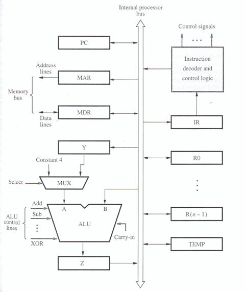
- Register Transfers: Moving data, say from R1 to R3, requires activating specific control signals.
R1outenables placing R1's content onto the internal bus.R3inenables loading data from the bus into R3. These transfers are synchronized by the processor clock, using input/output gating logic for each register bit. - ALU Operations: To perform an operation like
R3 ← [R1] + [R2], a sequence of steps is needed:R1out, Yin(Transfer R1's content to the temporary register Y, which feeds one ALU input).R2out, SelectY, Add, Zin(Place R2's content on the bus, select Y as the other ALU input via the MUX, command the ALU to perform addition, and latch the result into the temporary output register Z).Zout, R3in(Transfer the result from Z, via the bus, into the destination register R3).
- Memory Fetch: To read from memory location
LOCinto register R2:- The address
LOCis loaded into the MAR. - The
MARoutsignal places the address onto the memory bus, and theReadcontrol signal is asserted. - The processor typically waits (
WMFC) for aMemory Function Complete(MFC) signal back from the memory unit, indicating the data is ready. - The
MDRinEsignal enables loading the data from the memory bus into the MDR. MDRout, R2ingates the data from the MDR onto the internal bus and into register R2.
- The address
- Complete Instruction Example (
Add (R3), R1): This instruction adds the content of the memory location pointed to by R3, to register R1. The execution involves several steps combining the operations above: fetching the instruction, fetching the operand from the memory address stored in R3, performing the addition using R1 and the fetched operand, and storing the final result back in R1. A typical sequence might involve 7 distinct steps or clock cycles. - Branch Execution: An unconditional branch
Branch TARGETcalculates the target address, often as the current PC value plus an offset specified in the instruction (PC ← [PC] + Offset(TARGET)), and loads this new value into the PC. This usually takes about 2 steps after the instruction fetch.
(Question: What is the main disadvantage of the single-bus organization in terms of performance?) Answer: The single internal bus creates a bottleneck, as only one data transfer can occur at a time.
Multiple-Bus Organization
To overcome the single-bus bottleneck, multiple internal buses allow parallel data transfers, significantly improving performance. A common design uses three buses (e.g., Bus A, Bus B, Bus C).
- Structure: Such a structure allows, for instance, both ALU operands to be fetched simultaneously from the register file (which might be connected to Bus A and Bus B). The ALU output can then be directly routed via Bus C to the destination register. Often, a dedicated incrementer is included for the PC, allowing it to be updated in parallel with other ALU or data transfer operations.
- Execution Example (
Add R4, R5, R6): The three-bus organization allows this instruction to execute much faster than on a single-bus system. After fetching and decoding, the execution might only take one step:R4outA, R5outB, SelectA, Add, R6in, End(Simultaneously read R4 onto Bus A, R5 onto Bus B, perform the addition, and write the result from Bus C into R6). Compare this single execution step to the multiple steps needed for the ALU operation in the single-bus example.
This clearly shows the potential for performance improvement by allowing multiple transfers within a single clock cycle.
Generating Control Signals: The Control Unit
How does the processor generate the specific R1out, Yin, Add, Read, WMFC, End signals in the correct sequence for each instruction? This is the job of the Control Unit. There are two main approaches to designing it:
1. Hardwired Control
In this approach, the control signals are generated by dedicated combinational logic circuits, essentially fixed hardware logic.
- Organization: The control unit typically contains:
- Instruction Decoder: Interprets the opcode of the instruction currently in the IR.
- Step Decoder/Counter: Generates timing signals corresponding to the different steps (T1, T2, T3...) required for executing an instruction.
- Encoder Logic: Combines the decoded instruction information, the current timing step, status flags (condition codes), and external inputs (like the MFC signal) to generate the specific control signals needed for that step.
- Signal Generation: Each control signal (like
ZinorEnd) is produced by a specific Boolean logic expression. For example, the signal to latch data into the Z register (Zin) might be active during step T1 (for PC increment), or during step T6 of an ADD instruction, or during step T4 of a Branch instruction, and so on. Similarly, theEndsignal, which signifies the completion of an instruction, would be activated at the final step of each different instruction type (e.g., T7 for Add, T5 for Branch). - Pros & Cons:
- (+) Speed: Can operate very quickly as signals are generated directly by logic gates.
- (-) Complexity & Inflexibility: Difficult to design, test, and especially modify. Adding new instructions requires redesigning the hardware logic.
2. Microprogrammed Control
Here, the control signals needed for each step of each machine instruction are stored as patterns of bits (1s and 0s) in a special memory called the Control Store. Each pattern is a microinstruction or Control Word (CW).
- Concept: Executing a machine instruction involves fetching and executing a sequence of corresponding microinstructions (a microroutine) from the control store. Each microinstruction specifies which control signals should be active during one clock cycle.
- Example: The multi-step sequence for
Add (R3), R1would correspond to a microroutine of several microinstructions stored consecutively in the control store. The first microinstruction would have bits set to activatePCout,MARin,Read,Select4,Add,Zin. The next microinstruction would activateZout,PCin,Yin,WMFC, and so on. - Organization: A typical microprogrammed control unit includes:
- Control Store (CS): A fast memory (often ROM or PROM) holding the microinstructions.
- Micro-Program Counter (μPC): Holds the address of the next microinstruction to be fetched from the CS.
- Microinstruction Register (μIR): Holds the fetched microinstruction. The bits of the μIR directly drive the control lines of the datapath.
- Starting Address Generator: Maps the machine instruction's opcode (from the IR) to the starting address of its corresponding microroutine in the CS.
- Conditional Control: To handle decisions, microprogrammed control units allow conditional branching within the microroutines. Based on condition codes (like CPU flags N, Z, V, C) or external signals (like MFC), the next microinstruction fetched might not be the next sequential one; instead, the μPC can be loaded with a different address specified in the current microinstruction. This allows for loops (like waiting for MFC) and decision-making within the control sequence.
- Microinstruction Formats:
- Horizontal: Each bit in the microinstruction directly controls one signal. This leads to wide microinstructions but requires no decoding.
- Vertical/Encoded: Control signals are grouped into fields. For example, a 3-bit field could encode which of 8 registers should gate its output onto the bus. This results in narrower microinstructions but requires decoder circuits to generate the actual control signals from the fields. Most designs use some form of encoding.
- Sequencing: The μPC typically increments to fetch the next microinstruction. However, microinstructions can also specify:
- Branching: Unconditional or conditional jumps to other addresses within the control store.
- Next-Address Field: Some designs include the address of the next microinstruction directly within the current microinstruction, simplifying branching logic but increasing the size of each microinstruction.
- Pros & Cons:
- (+) Flexibility: Control logic can be changed by modifying the microprogram in the control store. This makes it easier to fix bugs or add new instructions. It also facilitates emulation (making one CPU architecture behave like another by writing a suitable microprogram).
- (-) Speed: Generally slower than hardwired control because of the time required to fetch microinstructions from the control store before generating the control signals.
(Debate: If you were designing a modern, high-performance CPU with a complex instruction set, would you lean towards hardwired or microprogrammed control? Why?) Answer: Many modern complex CPUs (like x86) use a hybrid approach. Simple, common instructions might be handled by hardwired logic for speed, while complex, less frequent instructions are interpreted by microcode.
Conclusion: Orchestrating Execution
The Basic Processing Unit is a marvel of coordinated activity. Whether using a single-bus or multiple-bus internal structure, the core function remains fetching and executing instructions step-by-step. The control unit, using either fixed logic (hardwired) or a flexible microprogram, generates the precise sequence of signals needed to manage register transfers, ALU operations, and memory interactions. Understanding these internal mechanisms is key to appreciating how computers translate high-level code into low-level actions.
Key Takeaways:
- Instruction execution involves fetch and execute phases, broken down into micro-operations like register transfers and ALU computations.
- Internal CPU organization (single-bus vs. multiple-bus) significantly impacts the potential for parallel operations and overall speed.
- Control signals, generated by the Control Unit, orchestrate all CPU actions.
- Hardwired control offers speed through dedicated logic but is inflexible.
- Microprogrammed control provides flexibility via stored microinstructions but is generally slower.